Our products are on European objectives

  1. To create beyond global state-of-the-art electronics and connectivity solutions enabling the digital transformation by designing Continium’s innovative, power saving data converters (ADC, DAC) for interfacing the analog domain. Our world is analogue (audio, video, sensoric, RF antenna signals) and data converters like ADC are the key electronic components to digitize the analog input signals for digital processing in computers. For example, in the RF wireless signal path’s ADCs are the most valuable elements, since their accuracy affects the overall system accuracy. Any ADC errors in form of non-linearity or distortions spurs or ADC noise can never be eliminated later in digital real-time processing. Data converters are limited by the counteracting fact of speed vs. accuracy, thus innovative CTSD ADC architectures have to be applied to digitize the GHz frequency signals for 5G/6G wireless systems. Without high performant European data converters there will be no digital transformation in Europe.
  2. To push for the most energy-efficient and resource-sharing electronics by drastically reducing power consumption of data converters by innovative research opposite to obsolete parallel Nyquist ADCs being supplied by giant semiconductor companies, to save energy and to help electronics to be more eco-friendly.
  3. To significantly increase the microelectronics manufacturing footprint for innovative products in Europe by designing innovative data converters in domestic European semiconductor technologies (e.g., X-FAB, GloFo, STmicro) avoiding expensive foreign 3nm-5nm FinFET technologies. By Continium’s “Differentiation by clever Design” using moderate technologies (e.g.22nm) we will introduce innovation in multichannel MIMO wireless systems and sensorics, potentiated by lowest power consumption and thus allow SMEs to manufacture innovative and competitive products. In this way Continium will strengthen the semiconductor value chain as well as generally Europe-based electronic manufacturability, means increasing the European manufacturing footprint.

Continium’s silicon IP cores

Select a product for more information:

20b-linear 100MS/s DAC

View more →

14b 30kS/s serial ADC

View more →

15b 4kS/s serial ADC

View more →

12b 1MS/s serial ADC

View more →

14b 560kS/s pipeline ADC

View more →

LiDAR: optical receiver amplifier

View more →

Wireless 5G base station transceiver

View more →

Universally reconfigurable 14-bit capacitive sensor interface

View more →

Exponential rising of ASIC R&D cost as semiconductor chips are approaching 5nm technology node
Mark LaPedus: Big Trouble at 3nm (21.June 2018)

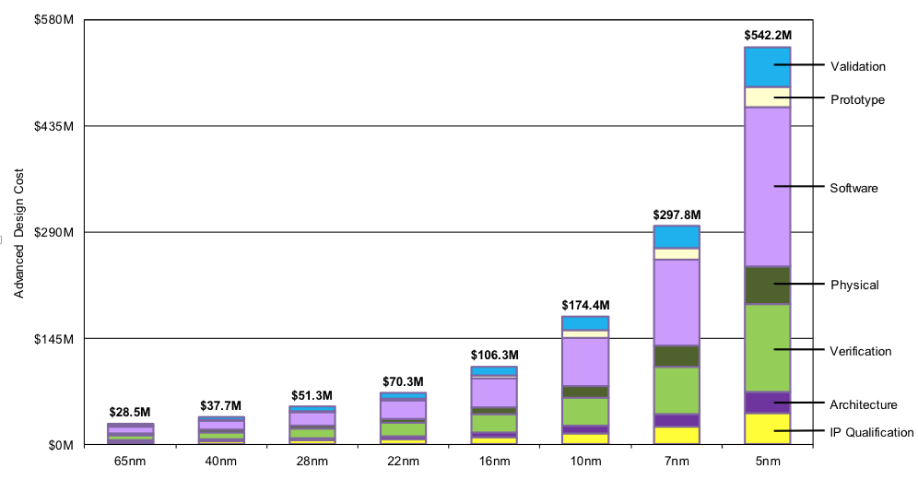
“Design costs are also a problem. Generally, IC design costs have jumped from $51.3 million for a 28nm planar CMOS device to $297.8 million for a 7nm FinFET chip and $542.2 million for 5nm FinFET, according to IBS. But at 3nm, IC design costs range from a staggering $500 million to $1.5 billion, according to IBS.For that reason, customers likely will stay at certain nodes longer, such as 22nm/16nm/14nm and 7nm, before even thinking about switching to 3nm. Some may never move to 3nm. And if or when gate-all-around appears, it may get pushed out beyond its target date of 2021.Design costs are also a problem. Generally, IC design costs have jumped from $51.3 million for a 28nm planar CMOS device to $297.8 million for a 7nm FinFET chip and $542.2 million for 5nm FinFET, according to IBS. But at 3nm, IC design costs range from a staggering $500 million to $1.5 billion, according to IBS.For that reason, customers likely will stay at certain nodes longer, such as 22nm/16nm/14nm and 7nm, before even thinking about switching to 3nm. Some may never move to 3nm. And if or when gate-all-around appears, it may get pushed out beyond its target date of 2021.”